High Temperature PCB: 8-Layer HDI Gold Finger Circuit Board with Gold-Plated Edge Connectors
(Custom PCBs are tailored products; the images and specifications provided are for reference only.)
General Description
This essay outlines an 8-layer printed circuit board (PCB) built on an FR-4 substrate with a Tg of 170°C, specifically designed for mobile broadband applications. The PCB has a thickness of 1.6 mm and features a white silkscreen (Taiyo) on a green solder mask (Taiyo) with immersion gold on the pads. It includes 80 strips of gold fingers on the edge for easy insertion. The base material is sourced from Taiwan's ITEQ, providing one PCB per panel. The design incorporates blind vias from the top layer to inner layer 6 and buried vias from inner layer 3 to inner layer 6. The fabrication adheres to IPC 6012 Class 2 standards using supplied Gerber data, with each shipment containing 25 boards.
Features and Benefits
High Tg Material: Offers excellent thermal reliability and resistance to CAF, ensuring long-term performance for industrial and automotive applications.
Gold Fingers: Significantly reduce contact resistance for better connectivity.
Large Workshop: 16,000 m² facility for efficient production.
Comprehensive Services: Supports your PCB needs from prototyping to mass production.
Strict Quality Control: Implemented WIP inspection and monitoring alongside thorough working instructions.
IPC Compliance: Manufactured according to IPC Class 2 and Class 3 standards.
Certifications: ISO9001, ISO14001, ISO13485, and UL certified manufacturing processes.
Flexible Shipping: Various shipping methods available, including FedEx, DHL, TNT, and EMS.
No Minimum Order Quantity: Low-cost options for prototypes and small runs.
PCB Specifications
| PCB SIZE | 150 x 141mm=1PCS |
| BOARD TYPE | Multilayer PCB |
| Number of Layers | 8 layers |
| Surface Mount Components | YES |
| Through Hole Components | NO |
| LAYER STACKUP | copper ------- 18um(0.5oz)+plate TOP layer |
| Prepreg 7628(43%) 0.195mm | |
| copper ------- 35um(1oz) MidLayer 1 | |
| FR-4 0.2mm | |
| copper ------- 35um(1oz) MidLayer 2 | |
| Prepreg 7628(43%) 0.195mm | |
| copper ------- 35um(1oz) MidLayer 3 | |
| FR-4 0.2mm | |
| copper ------- 35um(1oz) MidLayer 4 | |
| Prepreg 7628(43%) 0.195mm | |
| copper ------- 35um(1oz) MidLayer 5 | |
| FR-4 0.2mm | |
| copper ------- 35um(1oz) MidLayer 6 | |
| Prepreg 7628(43%) 0.195mm | |
| copper ------- 18um(0.5oz)+plate BOT Layer | |
| TECHNOLOGY | |
| Minimum Trace and Space: | 4mil/4mil |
| Minimum / Maximum Holes: | 0.35/3.5mm |
| Number of Different Holes: | 23 |
| Number of Drill Holes: | 183 |
| Number of Milled Slots: | 0 |
| Number of Internal Cutouts: | 0 |
| Impedance Control | no |
| Number of Gold finger | 39 |
| BOARD MATERIAL | |
| Glass Epoxy: | FR-4, ITEQ IT-180 TG170℃ er<5.4 |
| Final foil external: | 1oz |
| Final foil internal: | 1oz |
| Final height of PCB: | 1.6mm ±0.16 |
| PLATING AND COATING | |
| Surface Finish | Immersion gold on pad, electroplated gold on edge connectors |
| Solder Mask Apply To: | TOP and Bottom, 12micron Minimum |
| Solder Mask Color: | Gloss Green, Taiyo PSR-2000GT600D |
| Solder Mask Type: | LPSM |
| CONTOUR/CUTTING | Routing |
| MARKING | |
| Side of Component Legend | TOP and Bottom. |
| Colour of Component Legend | White, Taiyo IJR-4000 MW300 |
| Manufacturer Name or Logo: | Marked on the board in a conductor and leged FREE AREA |
| VIA | Plated through hole(PTH), Blind via, Buried vias |
| FLAMIBILITY RATING | UL 94-V0 Approval MIN. |
| DIMENSION TOLERANCE | |
| Outline dimension: | 0.0059" |
| Board plating: | 0.0029" |
| Drill tolerance: | 0.002" |
| TEST | 100% Electrical Test prior shipment |
| TYPE OF ARTWORK TO BE SUPPLIED | email file, Gerber RS-274-X, PCBDOC etc |
| SERVICE AREA | Worldwide, Globally. |
.jpg)
Typical Applications
Bluetooth Transmitters
HDMI Splitters
CCTV Systems
LED Street Lights
Low Noise Amplifiers
Door Access Control Systems
5G Mobile Hotspots
Multicouplers
Embedded Systems Development
Smartphones and Cell Phones
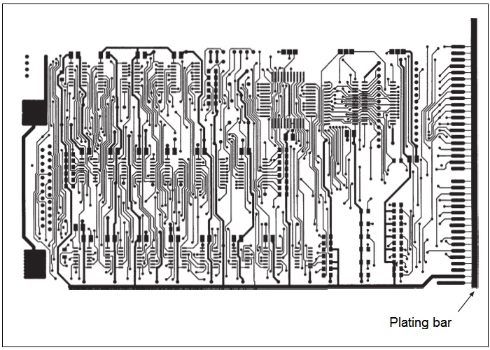
Gold Finger PCB
Gold fingers are designed to establish electrical connections without requiring a two-part connector system. The plating process involves electrolytic deposition of nickel and gold, similar to copper and tin/lead plating. Gold thickness can be controlled more precisely in automatic processes, ensuring consistency across contact fingers.
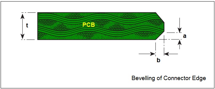
b
Edge connectors often feature guiding slots to prevent incorrect insertion, and the edges are beveled to ease insertion and reduce contact scraping during use.